Complex Digital, Analog & Power Supply designs
- Technical documentation
- Schematic Libraries
- Layout Footprints
- 3D Component libraries
- Simulation models
- Schematics
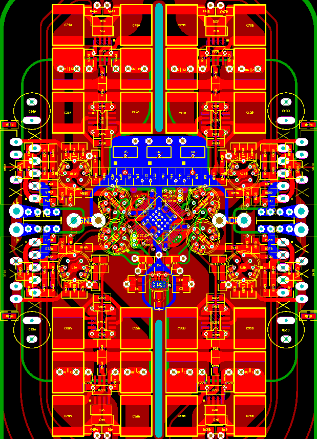
- Layout (PCB)
- Full manufacturing documentation – BOMs, Gerbers, PnP, Assembly Drawings, etc.
Design simulations
- Electrical simulations
- Thermal simulations
- Electromagnetic emission simulations
Exercising, tests & certified measurements
- Quality Assurance & Stability tests
- Radiated (EMI & RFI) and Conducted emission measurements
- EMC tests
- X-Ray inspection
- Optical inspection
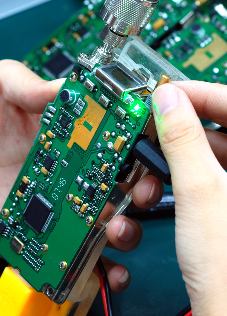
PCB Manufacturing, Assembling & Inspection
- Multi-layer PCBs with up to 30 layers
- Any components with extremely fine pitch
- Track thickness down to 3mils (0.075mm)
- Track-to-Track clearance down to 3mils (0.075mm)
- Inner via diameter down to 4mils (0.1mm)
- Blind and Buried vias
- Back drilling
- Hard Gold, ENIG & HAL
- Surface protection layers
- RoHS & Lead compliance
- Precise inspection
Ψ